Self-Assembled DNA-Based Structures for Nanoelectronics
Received 16 November 2012; Accepted 17 December 2012
Journal of Self-Assembly and Molecular Electronics, Vol. 1, 101–124.
doi: 10.13052/same2245-4551.115
Copyright © 2013 River Publishers. All rights reserved.
Veikko Linko1, J. Jussi Toppari2
- 1Physics Department, Walter Schottky Institute, Technische Universität München, 85748 Garching near Munich, Germany; e-mail: veikko.linko@tum.de
- 2Department of Physics, Nanoscience Center, University of Jyväskylä, P.O. Box 35, 40014 Jyväskylä, Finland; e-mail: j.jussi.toppari@jyu.fi
Abstract
Recent developments in structural DNA nanotechnology have made complex and spatially exactly controlled self-assembled DNA nanoarchitectures widely accessible. The available methods enable large variety of different possible shapes combined with the possibility of using DNA structures as templates for high-resolution patterning of nano-objects, thus opening up various opportunities for diverse nanotechnological applications. These DNA motifs possess enormous possibilities to be exploited in realization of molecular scale sensors and electronic devices, and thus, could enable further miniaturization of electronics. However, there are arguably two main issues on making use of DNA-based electronics: (1) incorporation of individual DNA designs into larger extrinsic systems is rather challenging, and (2) electrical properties of DNA molecules and the utilizable DNA templates themselves, are not yet fully understood. This review focuses on the above mentioned issues and also briefly summarizes the potential applications of DNA-based electronic devices.
Keywords
- Self-assembly
- DNA nanostructures
- electrical conductivity of DNA
- carbon nanotubes
- nanoparticles
1. Structural DNA Nanotechnology
Since Nadrian Seeman’s pioneering work in the beginning of 1980s [1], DNA has been considered as a promising material for nanoscale constructions due to its superior self-assembly characteristics, small size and suitable mechanical properties. The highly specific and predictable Watson-Crick base pairing of complementary base sequences of single-stranded DNA (ssDNA) molecules can be utilized in programming desired double-stranded DNA (dsDNA)-based motifs, which can be further assembled into larger and more complex structures. These DNA structures can also serve as templates for other nanoscale objects.
During recent decades, numerous different DNA structures have been introduced. The very first ones were based on flexible branched junctions [2], but the next generation of structures were already quite complex, comprised of more rigid motifs, such as double crossover (DX) and triple crossover (TX) tiles [3–6], where parallel DNA helices (two in DX and three in TX) are connected to each other via two strand-exchange points, i.e. crossovers. Later on, it was realized that structures could be formed also by using a long scaffold strand combined with shorter DNA fragments [7, 8]. In 2006, Paul Rothemund presented the DNA origami method [9], based on folding a long single-stranded scaffold strand into a desired shape with the help of a set of ssDNA staples (short oligonucleotides). This robust high-yield method has then been extended to three-dimensional shapes [10], resulting in the structures with stress [11] and complex curvatures [12, 13]. In addition, there exist efficient tools, which can help in designing and simulating the origami shapes [14–16]. The rapid progress and the future challenges of the field have been reviewed in [17, 18]. Very recently, a rapid folding of complex 3D origamis, with yields approaching 100%, has been introduced [19], as well as scaffold-free 2D and 3D architectures, which can act as molecular canvases for creating a huge number of distinct arbitrary shapes, with a fair yield [20, 21]. Moreover, it has been shown that the core of a densely packed origami can have a high-degree of structural order [22], thus supporting the idea of complex, high-resolution platforms for diverse applications. Therefore, all these recent achievements truly expand the possibilities in designing custom, spatially well controlled structures at even subnanometer scale.
The novel DNA designs open up opportunities in many distinct research fields, since the structures can be almost arbitrarily patterned with other nano-scale components such as carbon nanotubes [23], proteins [24, 25], metallic nanoparticles [26–29], and quantum dots [30]; not to mention that the structures could also be completely metallized [31–33]. With the help of a DNA template, the placement and orientation of individual molecules or larger molecular assemblies becomes possible, in principle with an accuracy of a single base pair (0.34 nm height, 2 nm helix diameter). For molecular electronics, it means that DNA architectures could serve as versatile molecular scale circuit boards, enabling fabrication of sophisticated nanodevices well below the 22 nm feature size – the next goal of semiconductor industry [34]. Besides the implicit high-resolution, these methods exploit parallel self-assembly processes and could thus provide cheaper and faster way to fabricate nanoscale devices in comparison to the standard top-down-based methods, and thus offer major advantages for the miniaturization of electronics [35, 36].
But could we really utilize DNA molecules as circuit boards? Or could even a DNA template itself behave as a conductor? What is the influence of the environment to a behavior of the fragile DNA? Understanding of electrical properties of DNA is important not only for molecular electronics, but also in a field of organic devices [37], medicine and cancer therapy as well as in investigation of genetic mutations and especially in biological sensing [38–40].
2. DNA in Electronics
2.1. Electrical Properties of Double-Stranded DNA
In 1962, it was first time suggested that dsDNA molecules could conduct electricity due to the overlapping π-orbitals of adjacent bases on the base pair stack [41]. Since then, and in particular during recent twenty years, huge amount of theoretical and experimental articles about DNA conductivity have been published: In 90’s the actual charge transfer (CT) from one base to another along the dsDNA helix was proven by chemical approach, within an aqueous buffer, by utilizing modified bases acting as a donor and acceptor while monitoring the quenching of the acceptor fluorescence after triggering the donor [42–44]. Since that there have been variety of studies about the DNA CT processes yielding a mixture of conclusions; the variation being mostly due to the differences in coupling of the donor and the acceptor within the base pair stack [45]. Usually CT studies have covered short distances, but also long range CT has been recently reported [40]. After the promising results based on chemical approach published in 1990s, a large variety of studies with physical approaches, i.e., directly measuring the conductivity of dsDNA, soon followed with contradicting results: insulating [31], ohmic [46], semiconducting [47], and even superconducting [48] properties have been reported. The conductivity can be sequence- and mismatch-dependent [40, 49], and it can also be a combination of nucleotide, backbone, and ion-based conductances [50]. Wide range of distinct and controversial results of dsDNA conductivity and the proposed conductance mechanisms (electronic coupling between π-orbitals of neighboring base pairs [41], tunneling or thermally induced hopping [45]) can be found in [51–53].
There also exist several factors that need to be taken into account in a measurement setup but are in most cases highly non-trivial to control. In many physical experiments the contacts between electrodes and DNA play a crucial role [54], while ensuring a proper electrical contact at a single molecule level is extremely difficult [55]. Further, even if the proper contacts could be realized, various environmental factors, e.g. humidity, can have an influence on the conformation of DNA [56], and also to the conductivity [57, 58]. At the high humidity levels the adsorbed and ionized water molecules surrounding the dsDNA can act as charge carriers [59, 60], or at higher frequencies the conductivity can be ascribed to relaxational losses of the surrounding water dipoles [61]. On the other hand, if electrical measurements are performed in a vacuum chamber, the DNA molecule should completely dehydrate resulting in an unknown conformation. In addition, the type of counter-ions and the salt concentration are known to have a large impact to the secondary structure of dsDNA, and ions can also diffuse and migrate along DNA, thus enhancing an ionic conductivity. Yet, the charge of a DNA molecule affecting to the amount of the counter-ions, depends on the dissociation of the phosphate groups and therefore on pH. The observed conductivity is also dependent on the measurement geometry (DNA lying on the substrate vs. freely hanging geometry) and the type of the substrate used, since the conformation of DNA also depends on the interaction between DNA and the substrate in question [62].
Nevertheless, today it seems to be quite clear that a really long, completely unmodified dsDNA molecule itself does not have high enough conductance for serving as an electrical building block or a wire, and equally, it is not sturdy enough to be used in electronic devices. Yet, the conductance mechanisms of DNA are not fully revealed and the topic of the conductivity of the dsDNA still remains highly controversial. Hence, it is not very well known whether other more complex forms of DNA could provide better properties for electronics, or if relatively rigid DNA constructs or some particular parts of them, could conduct electricity if appropriately designed. There already exist several studies on these issues, of which the former being briefly discussed in the next section. The conductivity of dsDNA-based nanostuctures, being one of the main topics of this review, will be reviewed in more detail in later sections to complete an overall picture of the status of the field.
2.2. Other Linear DNA Conformations
Since the conductivity of a plain long dsDNA molecule has been shown not to be sufficient for electronics, many other DNA conformations and derivates such as metallo-DNAs [63–65] or G-wires [66–69] have been studied. The metallo-DNA (M-DNA) is a derivative of dsDNA in which metal ions are incorporated between the bases by replacing the amino protons of guanine and thymine on each of the base pairs at high pH. The metal ions couple the energy levels of the adjacent bases and lower the energy gap, thus enhancing the conductivity of the dsDNA [65]. This enhanced conductivity has been observed already for Zn/M-DNA [63]. However, the conductivity is not drastically improved, and in general, delicate and well controlled environment is needed to sustain the form of M-DNA.
Besides the double-helix, certain sequences can also adopt three- or four-stranded conformations [70, 71]. Four-stranded conformation is especially stable for guanine-rich sequences in the presence of monovalent and/or divalent metal cations [71–73]. These long structures, named G-wires, are comprised of stacked tetrads arising from the planar association of four guanines by Hoogsteen bonding [74, 75]. G-wire is a promising candidate for an electrical conductor since it is sturdier compared to dsDNA and made solely of guanine, characterized by the lowest ionization potential among the DNA bases, thus likely to enable more efficient charge migration along DNA. There already exists clear experimental evidence of an electrostatic polarizability of the G-wires indicating possible electrical conductivity [67].
In addition to its presumably better conductivity and improved mechanical properties, the G-wire still possesses almost the same self-assembly properties as dsDNA, and thus, can be equally functionalized or modified [76]. Functionalization of G-wires with gold and silver nanoparticles to form stable complexes has already been demonstrated [77, 78], and moreover, plenty of ideas about nanoscale molecular machines utilizing G-rich strands and their conformation changes have been suggested [79–83].
2.3. DNA-Based Electronic Biodevices
Self-assembled DNA-based devices can also be exploited as electronic bio-sensors, e.g. for recognizing DNA and certain base sequences [35, 84–87]. The working principle of these sensors can be based on electrochemical detection [88], direct electrical signal [89, 90] or for example on a DNA field effect transistor (DNA-FET) [91], where the gate is made of ssDNA molecules acting as surface receptors for investigated molecules. The latter one is based on the change of the charge distribution in the vicinity of the gate when a target molecule hybridizes with the receptors, and thus the current between the drain and the source will be modulated.
Solid-state nanopores are often used for electronic detection of various types of molecules [92], but for some particular applications the pore size, properties and functionality of the opening should be accurately tuned. This can be achieved by incorporation of DNA structures into the pores, mimicking the idea of protein pores in solid-state openings [93]. Very recent examples show that the 3D DNA origami structures can serve as plugs [94] or gatekeepers [95] for the lithographically fabricated pores. These hybrid pores can be precisely controlled in size and shape, and are easily functionalized. In addition, the extension of these methods demonstrated origami pores attached even to lipid membranes [96]. It is highly possible that combination of DNA transistors with nanopore techniques will lead to a realization of devices allowing cheap DNA sequencing in the near future.
3. Placement of DNA Structures on a Chip
In order to reliably determine the conductance of DNA structures or make any use of them in molecular electronics, they have to be integrated to other circuitry in a controllable way. Naturally, there exist numerous possible ways to achieve this, and only some of the most studied and sufficient methods are discussed in the following sections.
3.1. Anchoring DNA Structures on Patterned or Chemically Modified Surfaces
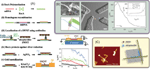
There exist many readily available chemical methods for positioning DNA-templates on the chip. One impressive example is to anchor DNA structures on lithographically fabricated wells according to their specific shape. Kershner et al. proposed and demonstrated how to attach triangular origamis to the origami-shaped binding sites etched in silicon oxide and diamond-like carbon substrates [97]. The followed extension of this method allowed one to organize gold nanoparticles on a chip with nanometer-scale resolution as shown in Figures 1A–C [98]. Besides the small feature size, this technique also provides high yield and enables a large scale assembly, thus being a candidate for commercial fabrication method of nanoelectronic devices in the future. Nanoparticles can also be assembled within the confined spaces with the help of patterned DNA strands in order to form surface-driven superlattices [99].
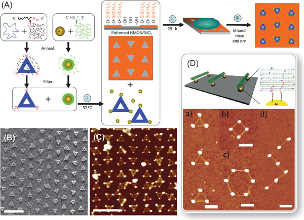
Figure 1 (A) Process for fabricating triangular DNA origamis with extra poly-adenine A30 strands extending from the corners, conjugating them with a poly-thymide functionalized gold nanoparticles (AuNP), and assembling two-dimensional nanoparticle arrays by utilizing triangular binding sites of clean oxide in a HMDS film patterned by electron-beam lithography [98]. The schematic illustrates the three key steps: (i) high-yield origami and AuNP binding, (ii) controlled DNA origami adsorption and (iii) ethanol treatment for drying and salt removal. (B) AFM image of triangular DNA origamis attached to the specific binding sites with a preferred orientation. The binding sites have sides of 110 nm and alternate between columns pointed up and columns pointed down. (C) AFM image of origamis bound with polyT-coated AuNPs and adsorbed to a similar substrate with binding site side length of 100 nm. Scale bars in (B) and (C) are 500 nm. (D) Schematic drawing of lithographically fabricated gold islands connected by DNA origami tubes on the substrate. Thiolated DNA strands (red) are extended from each end of the DNA origami tube thus aligning the tubes along the gold islands. The position of the thiolated groups is designed so that the tube can only connect the gold islands, if its length matches the distance between the islands [101]. Below are AFM images of various structures formed by connecting gold islands with DNA origami tubes. All scale bars are 300 nm. (A)–(C) adapted from [98] by permission from MacMillan Publishers Ltd., © 2009 Nature Publishing Group. (D) Adapted from [101] with permission, © 2010 American Chemical Society.
Other techniques for placement of DNA structures are often based on chemical attachment. Gerdon et al. used lithographically produced and 11-mercaptoundecanoic acid (MUA) modified areas on a chip for immobilizing origamis specifically, and furthermore positioning gold nanoparticles to the selected locations on top of the anchored origami [100]. There also exist other examples of chemicals suitable for controlled attachment of origamis on a substrate: hexamethyldisilazane (HMDS) prevents the attachment to certain areas [101, 102] and hydrogen silsesquioxane (HSQ) immobilizes origamis to the surfaces [103]. Lithographic methods (conventional or nanoimprint) can be utilized in patterning chemically selective binding areas on a large scale [101, 102, 104] or in fabrication of arrays of binding points attaching origamis selectively by the size as presented in Figure 1D [101, 105].
3.2. Trapping with Electric Fields
One of the most useful methods to direct and trap objects in solution is dielectrophoresis (DEP). It offers more dynamics and extra control on the trapping, if compared to the chemical or lithographical methods. DEP means a translational motion of a polarizable particle within an inhomogeneous electric field [106, 107]. The DEP force is proportional to the gradient of the square of the electric field, and the direction of the force depends on the polariz-ability of the particle compared to the surrounding medium. If the gradient and the difference in polarizabilities of the object and the medium are large enough, DEP can be utilized in manipulating materials even in nanoscale. Although the Brownian motion poses challenges in capturing of small objects from solution, various micro- and nanoscale objects have been successfully directed and trapped by DEP, and the method has been applied in variety of fields. DEP has largely been used as an active and non-destructive manipulation method for trapping cells, viruses, proteins and beads [108–110] as well as components directly exploitable for molecular electronics such as carbon nanotubes [111], nanoparticles [112, 113] and quantum dots [114] (see [115] for more complete review).

Figure 2 Trapping DNA origami with dielectrophoresis [123]. (A) AFM image of origami structures used for DEP trapping. The image is taken on a mica surface using tapping mode AFM in liquid. (B) Schematic view of the origami trapping using lithographically fabricated gold nanoelectrodes. The inset illustrates the electromagnetic forces (EMF) acting on a DNA and the principle of positive DEP. The DNA structures are also straightened during the DEP trapping. AFM image of a single smiley (C) and a rectangular origami (D) trapped with DEP (on SiO2 surface, tapping mode AFM in air). All the scale bars are 100 nm. Adapted with permission from [123], © 2008 Wiley.
In case of DNA, even short fragments can be efficiently trapped, since the DNA is surrounded by a highly polarizable counter-ion cloud in a solution [116, 117], making the trapping more efficient [118, 119]. There exist a huge number of examples of trapping of DNA molecules by dielectrophoresis – starting from Masao Washizu’s work in 1990s [120] – which are summarized in [119, 121, 122]. To average the electrophoretic forces due to the negative charge of DNA in aqueous buffer to zero, an AC voltage is usually utilized for trapping. By exploiting DEP-immobilization between nanoscale electrodes, DNA molecules can also be integrated and connected into the other circuitry.
The same methods can be equally applied to DNA-based structures. Kuzyk et al. showed that individual DNA origamis (smileys and rectangles [9]) can be trapped and immobilized to a silicon oxide chip in a controllable way by alternative current -DEP [123] as illustrated in Figure 2. The ∼12 MHz, ∼1 Vpp AC-voltage was applied to lithographically fabricated narrow fingertip-type gold nanoelectrodes, which yielded high enough gradient in the electrode gap for trapping the origamis. Origamis were thiol-modified in order to ensure a proper attachment to the electrodes via covalent sulphur-gold bonds. Trapping of the DNA origamis on a chip was the first reported DEP-manipulation of complex, designed self-assembled structures, proving DEP to be a truly adaptable technique for the purposes of molecular electronics.
Later on, similar DEP-based immobilization methods were utilized in characterization of electrical properties of distinct DNA constructs [124,125] (see Section 4). By using multiple electrode geometries, it has also been shown that DNA strands can be specifically immobilized only to selected electrodes [126]. This technique would enable complex wiring and bridging schemes of electrodes for creation of DNA networks [127], and prospectively, more sophisticated attachment and orientation of DNA templates on the chip could be realized.
4. Electrical Properties of DNA-Based Structures
As discussed above, it seems that dsDNA is a poor conductor. However, these results do not directly reveal the electrical properties of self-assembled dsDNA-based motifs. In Rothemund’s original article [9], the topology of the adjacent dsDNA-like components in DNA origami was not yet resolved. Only very recently, it was shown that DNA can actually have previously unobserved and unnatural topologies in the scaffolded densely packed structures [22]. Therefore, DNA motifs can also support slightly different base stacking than the natural dsDNA, and thus, also their conductivity properties can be distinct. Moreover, dsDNA segments within the core of the DNA constructs can be structurally very well shielded from the external environment by the neighboring strands, and that could also prevent excess dehydration and helical conformation from collapsing. Thus, the influence of the environment (water, ions) to strand conformation might significantly vary between spatially distinct segments of the object. Apart from this, the role of the crossovers (strand exchanges between the neighboring helices in DNA objects) in total conductance of the structure is also unclear.
Since the DNA structures have already shown to possess a huge potential as templates in the nanoscale patterning, their electrical properties should also be fully understood for realization of the prospective nanoelectronic applications. The following sections discuss in more detail the conductivity properties of DNA motifs based purely on dsDNA, as well as the fabrication and electrical characterization of DNA-templated CNT-transistors as an example of successful utilization of the motifs in organizing materials.

Figure 3 (A) Current-voltage characteristics before and after the deposition of the triangular DNA origami between the electrodes on the chip. Resistance before the deposition is ∼400 GΩ and after ∼20 GΩ. Imaginary (B) and real (C) part of the measured impedancies of an empty chip (dashed line), chip with DNA origami deposited (dotted line), and impedance of pure DNA origami (solid line) as a function of frequency calculated assuming parallel connection of the chip and the origami [128]. Adapted with permission from [128], © 2009 American Institute of Physics.
4.1. dsDNA-Based Motifs
The very first measurement of the electrical properties of DNA origami was reported in 2009, when Bobadilla et al. determined the current through variety of triangular origamis (not controlled number of structures) placed in the gap between voltage biased electrodes at ambient conditions [128]. The obtained DC-resistance of the parallel origamis was about 20 GΩ, as shown in Figure 3A. The group also measured the complex impedance within a wide range of frequencies. At low frequencies the impedance was high (similar to the DC-resistance) but was reduced with the increasing frequency reaching a significantly lower flat value at 100 kHz. Simultaneously the impedance turned from capacitive to resistive (see Figures 3B and C), suggesting that the DNA structures could be conductive in the high frequency region. It was also concluded that the conductivity of the DNA structures could not be determined alone or separately, since the attachment of origamis affect the conductance of the empty electrode arrangement as well.
The same group also measured a temperature dependence of the DC current-voltage characteristics of similar samples [129], revealing fully insulating behaviour below 240 K (resistance similar to the empty electrodes) and exponential dependency of the resistance with respect to the inverse of temperature close to the room temperature. In addition, the thermionic emission, as well as the hopping conduction models were fitted to the results yielding voltage dependent activation barriers ∼0.7 and ∼1.1 eV for low and high voltage regimes, respectively. Furthermore, the hopping was assigned as the main conductance mechanism close to the room temperature.
During the same year, Linko et al. characterized conductance mechanisms of single rectangular origamis [9] by utilizing DEP-immobilization described above [124]. A thiol-linker -modified and ligated [130] origami was immobilized between the nanoelectrodes (verified by AFM imaging), and both DC and AC characteristics were investigated at different relative humidity (RH) levels, since previous results suggested that distinct humidity conditions can have a huge influence to the conductivity of DNA [57–60]. At low RH levels the DNA origami was insulating with the resistance of the order of TΩ (similar resistance observed also for dry dsDNA [57]). At RH = 90%, DC-sweeping from −0.3 to 0.3 V produced non-linear current-voltage (I–V) curves with a resistance of 10 GΩ between −0.2 and 0.2 V, and about 2 GΩ outside this region as shown in Figure 4A. In comparison, the control sample (also underwent DEP, but without any DNA in the trapping buffer) yielded a linear I–V curve with a typical resistance value of 10–30 GΩ. Similar non-linear I–V characteristics have previously been reported also for dsDNA molecules, e.g. in [131, 132]. The high impedance of the DC measurement could be explained by the used hexanethiol-ssDNA linkers, as the resistance of hexanethiol has been reported to be from 10 MΩ to 1 GΩ [133] and, moreover, it has also been observed that a ssDNA molecule is a poor conductor [59]. The DC conductance was also determined as a function of RH, and the results indicated the conductance to be mostly ionic with a major contribution from the ionized water molecules [60, 134]. However, this observation could also be due to the highly resistive linkers conducting only via some water-assisted mechanism(s).
In addition, complex impedances of the same samples were measured at RH = 90% while varying the frequency of the AC bias voltage between 0.01 Hz and 100 kHz (Figures 4B and C). The AC impedance spectroscopy (AC-IS) results were modeled by equivalent circuits (Figures 4D and E) allowing one to identify distinct contributions to the total conductance [135]. The model was consistent with the DC data and also revealed that the resistance of the DNA origami or the DNA-assisted resistance in the gap region was about 70 MΩ. The measurement also showed that the conductance of a DNA origami in high humidity conditions is a combination of ohmic and ionic contributions and that the high impedance contacts can hide the actual conductance of an investigated object in the DC-measurements. This was the first demonstration of a fully detailed equivalent circuit modelling for DNA or single DNA structures. The model also reasonably agreed with the results by Bobadilla et al. [128] and Bellido et al. [129]: DC resistances were similar and dependent on water, and in both studies at room temperature the impedance was reduced significantly in the higher frequency regime again indicating water-assisted conductance. The observed results were also comparable to other works for dsDNA molecules, e.g. [136, 137].
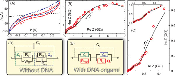
Figure 4 Impedance spectroscopy of a single rectangular DNA origami [124]. (A) Current-voltage characteristics of a control sample, underwent full DEP procedure except without DNA in the trapping buffer (black dotted line), and two samples containing single rectangular origamis between the electrodes (red solid line and blue dashed line). The hysteresis is due to the high humidity RH ≈ 90%. The direction of the voltage sweep is indicated by arrows. Cole-Cole plots of (B) control sample and (C) origami sample measured by impedance spectroscopy (red circles). The black lines are fittings of the equivalent circuits shown in (D) and (E). The arrows indicate the direction of increasing frequency. The inset in (C) is a blow out of the data near the origin. (D) Equivalent circuit for the control sample. Ce is the geometrical capacitance of the electrodes, and parallel combination of Rs , representing the small leakage current through the “electrolyte” (humid SiO2 surface), and Wdiff, describing the diffusion of the ions on the surface, forms the series impedance Zs (green). In series with this, there is the double-layer capacitance, Cdl, and Rct representing the current through it by redox reactions or tunneling. Together they form a double-layer impedance Zdl (blue). (E) Equivalent circuit for the origami sample includes the full control sample circuit, and additional components due to origami: resistance of the origami RDNA in parallel to Zs and contact of the origami to the electrode described by combination of resistance Rc and a constant phase element Qc in parallel to Zdl. This combination of Rc and Qc is a common way to describe many parallel connections with different time constants [135]. Adapted with permission from [124], © 2009 Wiley.
Since the conductance of DNA is known to drop with increasing length, similar AC-IS studies and modeling were performed for a shorter and smaller TX-tile-based molecular template [125]. This time hexanethiol-linkers were directly attached to the structure without low-conductance ssDNA linkers. However, the results showed that the impedance over the whole frequency range was higher than in the case of rectangular origamis. This observation might imply that the conductivity of DNA structures scales with the volume of the construct indicating water-induced or water-assisted conductivity along the DNA helices (polarised water molecules sheathing the DNA) to be the most probable charge transfer mechanism [59–61, 134].
In summary, the conductivity of the above-mentioned DNA structures (triangular and rectangular origamis and TX-tile-based objects) was found to be small suggesting that almost any kinds of devices for molecular electronics could be built on DNA without having to take the scaffold into account. The results indicate that the direct electronic conductivity via base pairs could be considered negligible in 2D DNA templates at least in the utilized setups and environments. This can simply be due to the non-optimal base stacking of the base pairs in a DNA structure [22, 40]. However, the conductance of 3D DNA structures still remains an open question. So far there is only one reported result of DNA-mediated CT in a 3D structure [138], but again, more results are expected soon.
4.2. DNA-Structures as Templates: CNT-Transistors
Despite the poor conductance of the reported sole DNA structures, various DNA templates can serve as nanoscale circuitboards for other electronic components, such as carbon nanotubes (CNTs), which are known to have suitable properties for molecular electronics and sensing [139]. Yet, it has been shown that, in addition to exploiting the DNA motifs in directing the CNTs to form molecular scale transistors [140–142], DNA can be also utilized in separation of different types of CNTs [143–145]. By combining these properties one can form an efficient tool-set for fabrication of CNT-transistors.
About a decade ago Keren et al. were the first ones to demonstrate the fabrication of a DNA-templated CNT-FET [146]. For a template they utilized a single dsDNA molecule, since more robust DNA motifs like origamis were not yet invented. The starting point in the fabrication was ∼200 nm long RecA modified ssDNA, which was hybridized to a selected point of much longer dsDNA template via homologous recombination [147]. Subsequently, biotinylated antibodies were attached to the RecA proteins, thus forming a chain of biotin binding sites. A streptavidin (STV)-coated CNT was then attached to these sites, and finally the parts of the dsDNA without RecA modification were chemically metallized yielding gold electrodes attached to the both ends of the CNT. The whole fabrication process is illustrated in Figure 5A.
Figure 5 (A) Step by step assembly of a DNA-templated CNT-FET (i)–(v) [146]. Schematic representation of the electrical measurement circuit, and measured electrical characteristics: drain-source current (IDS) versus gate voltage (VG) for different values of drain-source bias: VDS = 0.5 V (black), 1 V (red), 1.5 V (green), 2 V (blue). (B) Electrical characterization of a self-assembled CNT cross-junction [23]. Left: AFM image of a CNT cross-junction, and its schematic presentation on the ribbon (dark green) modified origami (grey). Middle: AFM amplitude image of the cross-junction with electron-beam patterned electrodes. The DNA template is no longer visible. Scale bars are 100 nm. Right: Source-drain current (ISD)versus CNT gate voltage (VG) for a source-drain bias of 0.85 V. Inset shows the source-drain I–Vsfor different gate voltages. (C) AFM image and schematics of a CNT assembly on DNA origami template using STV-biotin interaction [148]. CNTs wrapped with biotinmodified ssDNA were immobilized via STV on the origami templates with a certain pattern of biotin modifications. Adapted with permission: (A) from [146], © 2003 American Association for the Advancement of Science, (B) from [23], © 2009 Nature Publishing Group, and (C) from [148], © 2011 Wiley.
After fabrication, the DNA-templated CNT-FETs were mapped by AFM imaging and the gold electrodes were contacted by electron beam lithography, which allowed direct measurement of the devices, as illustrated in Figure 5A. The silicon substrate performed as a common gate electrode for all the devices on the same chip. In the same figure the measured current as a function of the gate voltage is represented for different bias (drain-source) voltages. The curves show clearly p-type FET behavior, typical for most CNT-FETs at ambient conditions. This result clearly proves the applicability of DNA-based fabrication process via self-assembly. Only drawback in the process was the high contact resistance between the CNT and the gold electrodes, which is due to a mismatch between the gold work function and the CNT energy levels, inducing the undesired saturation of the current at highly negative gate voltages, as visible in Figure 5A.
Later on, the DNA origami has been exploited in organization of two CNTs to form a cross-junction [23, 148]. Maune et al. used nucleotide-modified CNTs and attached them to both sides of a rectangular origami [9] via short DNA overhangs attained as perpendicular rows on the origami by extensions of the staple strands pointing out from the origami template [23]. However, the CNT attachment was successful only after extending the origami to a ribbon as shown in Figure 5B.
After depositing on a SiO2 covered silicon substrate, CNTs were connected by lithographically fabricated Au/Pt electrodes. Palladium (Pt) was chosen to minimize the contact resistance due to the work function, and furthermore, the exposed ends of the CNTs were chemically cleaned from DNA before depositing the metal. The applicability of the formed cross-junction as a transistor was demonstrated by characterizing its electrical properties using one CNT as a current channel of the FET and other as a gate. In total, six CNT-FETs were fabricated. Current-voltage characteristics measured from one of the FETs are shown as an example in the inset of the right panel of the figure 5B with different gate voltages. The main frame illustrates the observed gate voltage dependence revealing again the typical p-type behaviour. In this case the saturation at higher negative voltages was absent due to the smaller contact resistance.
Recently, Eskelinen et al. demonstrated an alternative and efficient method – based on biotin-STV interaction – for forming a similar CNT cross-junction on a DNA origami [148]. In that study, certain locations of the DNA origami were functionalized with biotin and followed by STV attachment. The formed streptavidin pattern again allowed biotinylated ssDNA-wrapped CNTs to be attached and aligned on the DNA template as shown in Figure 5C.
Apart from successful templating of CNT-transistors, DNA origamis have also been shown to be suitable platforms for creating plasmonic structures [28], for imaging and analyzing of single molecules [149–151], and for guiding chemical reactions [24], just to mention a few examples. Many more applications are foreseen.
5. Summary and Outlook
DNA has indeed proven to offer an ever increasing variety of possibilities to be utilized in fabrication of nanoscale structures. Its striking self-assembly capabilities has driven researchers to develop more and more novel ideas, driving the whole field through a major maturation; during the last two decades a development from the delicate tile-based systems to more robust origami-based methods has been witnessed. These approaches based on exploiting the exceptional self-assembly characteristics of DNA can serve as a toolbox for the next generation of device fabrication enabling the production of nanostructures made of materials relevant for electronics, optics and sensing. By combining the efficient and controllable DEP manipulation and chemical as well as geometrical placement methods of complex DNA constructs with the top-down techniques one can fabricate sophisticated and highly ordered circuits and functional devices truly in molecular scale.
In most cases the conductivity of the DNA scaffold could be considered negligible when used to assemble other molecular components. However, the conductivity of the DNA itself is still not fully untangled. Doping with metal ions, or on the other hand, the new forms of DNA, like G-wires; or even a recently discovered plasmon-initiated long range excitation transfer along a dsDNA [152], might open up opportunities for realizing novel DNA-based devices. Thus, the story of self-assembled DNA-based structures for molecular electronics is not yet fully written.
Acknowledgements
Financial support from Academy of Finland (Project Nos. 218182 and 263262) is greatly acknowledged. V.L. thanks the Emil Aaltonen Foundation. J.J.T. thanks NewIndigo ERA-NET NPP2 (AQUATEST, INDIGO-DST1-012) and EU’s COST action MP0802 for enabling fruitful collaborations.
References
[1] N. C. Seeman, J. Theor Biol., 99, 237–247 (1982).
[2] N. R. Kallenbach, R.-I. Ma, N. C. Seeman Nature, 305, 829–831 (1983).
[3] E. Winfree, F. Liu, L. A. Wenzler, N. C. Seeman Nature, 394, 539–544 (1998).
[4] H. Yan, S. H. Park, G. Finkelstein, J. H. Reif, T. H. LaBean Science, 301, 1882–1884 (2003).
[5] P. W. K. Rothemund, A. Ekani-Nkodo, N. Papadakis, A. Kumar, D. K. Fygenson, E. Winfree, J. Am. Chem. Soc., 126, 16344–16352 (2004).
[6] P. W. K. Rothemund, N. Papadakis, E. Winfree PLoS Biol., 2, e424 (2004).
[7] H. Yan, T. H. LaBean, L. Feng, J. H. Reif Proc. Natl. Acad. Sci. U.S.A., 100, 8103–8108 (2003).
[8] W. M. Shih, J. D. Quispe, G. F. Joyce Nature, 427, 618–621 (2004).
[9] P. W. K. Rothemund Nature, 440, 297–302 (2006).
[10] S. M. Douglas, H. Dietz, T. Liedl, B. Högberg, F. Graf, W. M. Shih Nature, 459, 414–418 (2009).
[11] T. Liedl, B. Högberg, J. Tytell, D. E. Ingber, W. M. Shih Nat. Nanotechnol., 5, 520–524 (2010).
[12] H. Dietz, S. M. Douglas, W. M. Shih Science, 325, 725–730 (2009).
[13] D. Han, S. Pal, J. Nangreave, Z. Deng, Y. Liu, H. Yan Science, 332, 342–346 (2011).
[14] S. M. Douglas, A. H. Marblestone, S. Teerapittayanon, A. Vasquez, G. M. Church, W. M. Shih Nucleic Acid Res., 37, 5001–5006 (2009).
[15] C. E. Castro, F. Kilchherr, D.-N. Kim, E. Lin Shiao, T. Wauer, P. Wortmann, H. Dietz Nat. Meth., 8, 221–229 (2011).
[16] D.-N. Kim, F. Kilchherr, H. Dietz, M. Bathe Nucleic Acid Res., 40, 2862–2868 (2012).
[17] A. V. Pinheiro, D. Han, W. M. Shih, H. Yan Nat. Nanotechnol., 6, 763–772 (2011).
[18] T. Tørring, N. V. Voigt, J. Nangreave, H. Yan, K. V. Gothelf Chem. Soc. Rev., 40, 5636–5646 (2011).
[19] J.-P. J. Sobczak, T. G. Martin, T. Gerling, H. Dietz Science, 338, 1458–1461 (2012).
[20] B. Wei, M. Dai, P. Yin Nature, 485, 623–626 (2012).
[21] Y. Ke, L. L. Ong, W. M. Shih, P. Yin Science, 338, 1177–1183 (2012).
[22] X.-c. Bai, T. G. Martin, S. H. W. Scheres, H. Dietz Proc. Natl. Acad. Sci. U.S.A., 109, 20012–20017 (2012).
[23] H. T. Maune, S. Han, R. D. Barish, M. Bockrath, W. A. Goddard III, P. W. K. Rothemund, E. Winfree Nat. Nanotechnol., 5, 61–66 (2010).
[24] N. V. Voigt, T. Tørring, A. Rotaru, M. F. Jacobsen, J. B. Ravnsbæk, R. Subramani, W. Mamdouh, J. Kjems, A. Mokhir, F. Besenbacher, K. V. Gothelf Nat. Nanotechnol., 5, 200–203 (2010).
[25] A. Kuzyk, K. T. Laitinen, P. Törmä Nanotechnology, 20, 235305 (2009).
[26] R. Schreiber, S. Kempter, S. Holler, V. Schüller, D. Schiffels, S. S. Simmel, P. C. Nickels, T. Liedl Small, 7, 1795–1799 (2011).
[27] M. R. Jones, K. D. Osberg, R. J. Macfarlane, M. R. Langille, C. A. Mirkin Chem. Rev., 111, 3736–3827 (2011).
[28] A. Kuzyk, R. Schreiber, Z. Fan, G. Pardatscher, E.-M. Roller, A. Högele, F. C. Simmel, A. O. Govorov, T. Liedl Nature, 483, 311–314 (2012).
[29] S. J. Tan, M. J. Campolongo, D. Luo, W. Cheng Nat. Nanotechnol., 6, 268–276 (2011).
[30] R. Wang, C. Nuckolls, S. J. Wind Angew. Chem. Int. Ed., 51, 11325–11327 (2012).
[31] E. Braun, Y. Eichen, U. Sivan, G. Ben-Yoseph Nature, 391, 775–778 (1998).
[32] J. Liu, Y. Geng, E. Pound, S. Gyawali, J. R. Ashton, J. Hickey, A. T. Woolley, J. N. Harb ACS Nano, 5, 2240–2247 (2011).
[33] Y. Geng, J. Liu, E. Pound, S. Gyawali, J. N. Harb, A. T. Woolley, J. Mater Chem., 21, 12126–12131 (2011).
[34] International Technology Roadmap for Semiconductors 2011 Edition, http://www.itrs.net/Links/2011ITRS/Home2011.htm
[35] A. Csáki, G. Maubach, D. Born, J. Reichert, W. Fritzsche Single Mol., 3, 275–280 (2002).
[36] K. Galatsis, K. L. Wang, M. Ozkan, C. S. Ozkan, Y. Huang, J. P. Chang, H. G. Monbouquette, Y. Chen, P. Nealey, Y. Botros Adv. Mater., 22, 769–778 (2010).
[37] K. Sakakibara, J. P. Hill, K. Ariga Small, 7, 1288–1308 (2011).
[38] J. Retèl, B. Hoebee, J. E. Braun, J. T. Lutgerink, E. van den Akker, A. H. Wanamarta, H. Joenje, M. V. Lafleur Mutat. Res., 299, 165–182 (1993).
[39] C. Dekker, M. Ratner Phys. World, 14, 29–33 (2001).
[40] J. D. Slinker, N. B. Muren, S. E. Renfrew, J. K. Barton Nat. Chem., 3, 228–233 (2011).
[41] D. D. Eley, D. I. Spivey Trans. Faraday Soc., 58, 411–415 (1962).
[42] C. J. Murphy, M. R. Arkin, Y. Jenkins, N. D. Ghatlia, N. J. Turro, J. K. Barton Science, 262, 1025–1029 (1993).
[43] T. J. Meade, J. F. Kayyem Angew. Chem. Int. Ed., 34, 352–354 (1995).
[44] F. Lewis, T. Wu, Y. Zhang, R. Letsinger, S. Greenfield, M. Wasielewski Science, 277, 673–676 (1997).
[45] E. M. Boon, J. K. Barton Curr. Opin. Struct. Biol., 12, 320–329 (2002).
[46] H.-W. Fink, C. Schönenberger Nature, 398, 407–410 (1999).
[47] D. Porath, A. Bezryadin, S. de Vries, C. Dekker Nature, 403, 635–638 (1999).
[48] A. Y. Kasumov, M. Koziak, S. Guéron, B. Reulet, V. T. Volkov, D. V. Klinov, H. Bouchiat Science, 291, 280–282 (2001).
[49] X. Guo, A. A. Gorodetsky, J. Hone, J. K. Barton, C. Nuckolls Nat. Nanotech., 3, 163–167 (2008).
[50] E. Shapir, H. Cohen , A, Calzolari , C. Cavazzoni, D. A. Ryndyk , G. Cuniberti, A. Kotlyar , R. Di Felice, D. Porath Nat. Mater., 7, 68–74 (2008).
[51] R. G. Endres, D. L. Cox, R. R. P. Singh Rev. Mod. Phys., 76, 195–214 (2004).
[52] D. Porath, G. Cuniberti, R. Di Felice Top Curr. Chem., 237, 183–228 (2004).
[53] M. Di Ventra, M. Zwolak Encycl. of Nanosci. and Nanotechnol., 2, 475–493 (2004).
[54] K. W Hipps Science, 294, 536–537 (2001).
[55] X. Guo, J. P. Small, J. E. Klare, Y. Wang, M. S. Purewal, I. W. Tam, B. Hee Hong, R. Caldwell, L. Huang, S. O’Brien, J. Yan, R. Breslow, S. J. Wind, J. Hone, P. Kim, C. Nuckolls Science, 311, 356–358 (2006).
[56] J. M. Warman, M. P. deHaas, A Rupprecht Chem. Phys. Lett., 249, 319–322 (1996).
[57] S. Tuukkanen, A. Kuzyk, J. J. Toppari, V. P. Hytönen, T. Ihalainen, P. Törmä Appl. Phys. Lett., 87, 183102 (2005).
[58] J. Berashevich, T. Chakraborty, J. Phys. Chem. B, 112, 14083–14089 (2008).
[59] T. Kleine-Ostmann, C. Jördens, K. Baaske, T. Weimann, M. H. de Angelis, M. Koch Appl. Phys. Lett., 88, 102102 (2006).
[60] C. Yamahata, D. Collard, T. Takekawa, M. Kumemura, G. Hashiguchi, H. Fujita Biophys. J., 94, 63–70 (2008).
[61] M. Briman,N.P.Armitage, E.Helgren, G.Grüner Nano Lett., 4, 733–736 (2004).
[62] A. Y. Kasumov, D. V. Klinov, P.-E. Roche, S. Guéron, H. Bouchiat Appl. Phys. Lett., 84, 1007 (2004).
[63] Y.-T. Long, C.-Z. Li, H.-B. Kraatz, J. S. Lee Biophys. J., 84, 3218–3225 (2003).
[64] S. Liu, G. H. Clever, Y. Takezawa, M. Kaneko, K. Tanaka, X. Guo, M. Shionoya Angew. Chem. Int. Ed., 50, 8886–8890 (2011).
[65] E. Shapir, G. Brancolini, T. Molotsky, A. B. Kotlyar, R. Di Felice, D. Porath Adv. Mater., 23, 4290–4294 (2011).
[66] A. B. Kotlyar, N. Borovok, T. Molotsky, H. Cohen, E. Shapir, D. Porath Adv. Mater., 17, 1901–1905 (2005).
[67] H. Cohen,T. Shapir, N. Borovok, T. Molotsky, R. Di Felice, A. B. Kotlyar, D. Porath Nano Lett., 7, 981–986 (2007).
[68] E. Shapir, L. Sagiv, T. Molotsky, A. B. Kotlyar, R. Di Felice, D. Porath, J. Phys. Chem. C, 114, 22079–22084 (2010).
[69] P. B. Woiczikowski, T. Kubar, R. Gutiérrez, G. Cuniberti, M. Elstner, J. Chem. Phys., 133, 035103 (2010).
[70] V. N. Soyfer, V. N. Potaman in Triple-Helical Nucleic Acids (Springer, New York, 1995).
[71] G. N. Parkinson, M. P. Lee, S. Neidle Nature, 417, 876–880 (2002).
[72] W. J. Qin, L. Y. Yung Nucleic Acids Res., 35, e111 (2007).
[73] N. Borovok, N. Iram, D. Zikich, J. Ghabboun, G.I. Livshits, D. Porath, A. B. Kotlyar Nucleic Acids Res., 36, 5050–5060 (2008).
[74] J. R. Williamson, M. K. Raghuraman, T. R. Cech Cell, 59, 871–880 (1989).
[75] J. T. Davis Angew. Chem., Int. Ed. Engl., 43, 668–698 (2004).
[76] S. Lyonnais, O. Piétrement, A. Chepelianski, S. Guéron, L. Lacroix, E. Le Cam, J.-L. Mergny Nucl. Acids Symp. Ser., 52, 689–690 (2008).
[77] I. Lubitz, A. B. Kotlyar Bioconjugate Chem., 22, 482–487 (2011).
[78] C. Leiterer, A. Csáki, W. Fritzsche Methods and Protocols, Series: Methods in Molecular Biology, 749, 141–150. Eds: Giampaolo Zuccheri and Bruno Samorì (Humana Press, Springer, 2011).
[79] P. Alberti, J.-L. Mergny Proc. Natl. Acad. Sci., 100, 1569–1573 (2003).
[80] R. P. Fahlman, M. Hsing, C. Sporer-Tuhten, D. Sen Nano Lett., 3, 1073–1078 (2003).
[81] Z. S. Wu, C. R. Chen, G. L. Shen, R. Q. Yu Biomater., 29, 2689–2696 (2008).
[82] B. Ge, Y. C. Huang, D. Sen, H.-Z. Yu Angew. Chem. Int. Ed., 49, 9965–9967 (2010).
[83] X. Yang, D. Liu, P. Lu, Y. Zhangc, C. Yu Analyst, 135, 2074–2078 (2010).
[84] W. Fritzsche, T. A. Taton Nanotechnology, 14, R63 (2003).
[85] E. Souteyrand, J. P. Cloarec, J. R. Martin, C. Wilson, I. Lawrence, S. Mikkelsen, M. F. Lawrence J. Phys. Chem. B, 101, 2980–2985 (1997).
[86] J. Fritz, E. B. Cooper, S. Gaudet, P. K. Sorger, S. R. Manalis Proc. Natl. Acad. Sci. U.S.A., 99, 14142–14146 (2002).
[87] Z. Li, Y. Chen, X. Li, T. I. Kamins, K. Nauka, R. S. Williams Nano Lett., 4, 245–247 (2004).
[88] E. E. Ferapontova, K. V Gothelf Curr. Org. Chem., 15, 498–505 (2011).
[89] S.-J. Park, T. A. Taton, C. A. Mirkin Science, 295, 1503–1506 (2002).
[90] R. Moeller and W. Fritzsche IEE Proc.-Nanobiotechnol., 152, 47–51 (2005).
[91] N. Mohanty, V. Berry Nano Lett., 8, 4469–4476 (2008).
[92] C. Dekker Nat. Nanotechnol., 2, 209–215 (2007).
[93] A. R. Hall, A. Scott, D. Rotem, K. K. Mehta, H. Bayley, C. Dekker Nat. Nanotechnol., 5, 874–877 (2010).
[94] N. A. W. Bell, C. R. Engst, M. Ablay, G. Divitini, C. Ducati, T. Liedl, U. F. Keyser Nano Lett., 12, 512–517 (2012).
[95] R. Wei, T. G. Martin, U. Rant, H. Dietz Angew. Chem. Int. Ed., 51, 4864–4867 (2012).
[96] M. Langecker, V. Arnaut, T. G. Martin, J. List, S. Renner, M. Mayer, H. Dietz, F. C. Simmel Science, 338, 932–936 (2012).
[97] R. J. Kershner, L. D. Bozano, C. M. Micheel, A. M. Hung, A. R. Fornof, J. N. Cha, C. T. Rettner, M. Bersani, J. Frommer, P. W. K. Rothemund, G. M. Wallraff Nat. Nanotechnol., 4, 557–561 (2009).
[98] A. M. Hung, C. M. Micheel, L. D. Bozano, L. W. Osterbur, G. M. Wallraff, J. N. Cha Nat. Nanotechnol., 5, 121–126 (2010).
[99] H. Noh, A. M. Hung, J. N. Cha Small, 7, 3021–3025 (2011).
[100] A. E. Gerdon, S. S. Oh, K. Hsieh, Y. Ke, H. Yan, H. T. Soh Small, 5, 1942–1946 (2009).
[101] B. Ding, H. Wu, W. Xu, Z. Zhao, Y. Liu, H. Yu, H. Yan Nano Lett., 10, 5065–5069 (2010).
[102] E. Penzo, R. Wang, M. Palma, S. J. Wind J. Vac. Sci. Technol. B, 29, 06F205 (2011).
[103] F. A. Shah, K. N. Kim, M. Lieberman, G. H. Bernstein J. Vac. Sci. Technol. B, 30, 011806 (2012).
[104] M. Palma, J. J. Abramson, A. A. Gorodetsky, E, Penzo, R. L. Gonzalez, Jr., M. P. Sheetz, C. Nuckolls, J. Hone, S. J. Wind J. Am. Chem. Soc., 133, 7656–7659 (2011).
[105] A. C. Pearson, E. Pound, A. T. Woolley, M. R. Linford, J. N. Harb, R. C. Davis Nano Lett., 11, 1981–1987 (2011).
[106] H. A. Pohl J. Appl. Phys., 22, 869–871 (1951).
[107] H. A. Pohl in Dielectrophoresis: The Behavior of Neutral Matter in Nonuniform Electric Fields (Cambridge Univesity Press, Cambridge, UK, 1978).
[108] M. P. Hughes Nanotechnology, 11, 124–132 (2000).
[109] P. J. Burke Encycl. of Nanosci. and Nanotechnol., 6, 623–641 (2004).
[110] L. Zheng, J. P. Brody, P. J. Burke Biosens. Bioel., 20, 606–619 (2004).
[111] A. Vijayaraghavan, S. Blatt, D. Weissenberger, M. Oron-Carl, F. Hennrich, D. Gerthsen, H. Hahn, R. Krupke Nano. Lett., 7, 1556–1560 (2007).
[112] R. Kretschmer, W. Fritzsche Langmuir, 20, 11797-11801 (2004).
[113] S. Kumar, Y.-K. Seo, G.-H. Kim Appl. Phys. Lett., 94, 53104 (2009).
[114] T. K. Hakala, V. Linko, A.-P. Eskelinen, J. J. Toppari, A. Kuzyk, P. Törmä Small, 5, 2683–2686 (2009).
[115] A. Kuzyk Electrophoresis, 32, 2307–2313 (2011).
[116] H. P. Schwan, G. Schwarz, J. Maczuk, H. Pauly J. Phys. Chem., 66, 2626–2636 (1962).
[117] S. Suzuki, T. Yamanashi, S. Tazawa, O. Kurosawa, M. Washizu IEEE Trans. Ind. Appl., 34, 75–83 (1998).
[118] S. Tuukkanen, A. Kuzyk, J. J. Toppari, H. Häkkinen, V. P. Hytönen, E. Niskanen, M. Rinkiö, P. Törmä Nanotechnology, 18, 295204 (2007).
[119] R. Hölzel IET Nanobiotechnol., 3, 28–45 (2009).
[120] M. Washizu, O. Kurosawa IEEE Trans. Ind. Appl., 26, 1165–1172 (1990).
[121] R. Hölzel, F. F. Bier IEE Proc.: Nanobiotechnol., 150, 47–53 (2003).
[122] A. Kuzyk, J. J. Toppari, P. Törmä Methods and Protocols, Series: Methods in Molecular Biology, 749, 223–234. Eds: Giampaolo Zuccheri and Bruno Samorì (Humana Press, Springer, 2011).
[123] A. Kuzyk, B. Yurke, J. J. Toppari, V. Linko, P. Törmä Small, 4, 447–450 (2008).
[124] V. Linko, S.-T. Paasonen, A. Kuzyk, P. Törmä, J. J. Toppari Small, 5, 2382–2386 (2009).
[125] V. Linko, J. Leppiniemi, S.-T. Paasonen, V. P. Hytönen, J. J. Toppari Nanotechnology, 22, 275610 (2011).
[126] V. Linko, J. Leppiniemi, B. Shen, E. Niskanen, V. P. Hytönen, J. J. Toppari Nanoscale, 3, 3788–3792 (2011).
[127] Y. Eichen, E. Braun, U. Sivan, G. Ben-Yoseph Acta Polym., 49, 663–670 (1998).
[128] A. D. Bobadilla, E. P. Bellido, N. L. Rangel, H. Zhong, M. L. Norton, A. Sinitskii, J. M. Seminario J. Chem. Phys., 130, 171101 (2009).
[129] E. P. Bellido, A. D. Bobadilla, N. L. Rangel, H. Zhong, M. L. Norton, A. Sinitskii, J. M. Seminario Nanotechnology, 20, 175102 (2009).
[130] P. O’Neill, P. W. K. Rothemund, A. Kumar, D. K. Fygenson Nano Lett., 6, 1379–1383 (2006).
[131] H. Cohen, C. Nogues, R. Naaman, D. Porath Proc. Natl. Acad. Sci, U.S.A., 102, 11589–11593 (2005).
[132] A. Rakitin, P. Aich, C. Papadopoulos, Y. Kobzar, A. S. Vedeneev, J. S. Lee, J. M. Xu Phys. Rev. Lett., 86, 3670–3673 (2001).
[133] B. Xu, N. J. Tao Science, 301, 1221–1223 (2003).
[134] D. H. Ha, H. Nham, K.-H. Yoo, H. So, H.-Y. Lee, T. Kawai Chem. Phys. Lett., 355, 405–409 (2002).
[135] E. Barsoukov, J. R. MacDonald in Impedance Spectroscopy: Theory, Experiment, and Applications, Second Edition (Wiley, Hoboken, New Jersey, 2005).
[136] J. Wang Phys. Rev. B, 78, 245304 (2008).
[137] B. Xu, P. Zhang, X. Li, N. Tao Nano Lett., 4, 1105–1108 (2004).
[138] N. Lu, H. Pei, Z. Ge, C. R. Simmons, H. Yan, C. Fan J. Am. Chem. Soc., 134, 13148–13151 (2012).
[139] J. Kong, N. R. Franklin, C. Zhou, M. G. Chapline, S. Peng, K. Cho, H. Dai Science, 287, 622–625 (2000).
[140] S. Lyonnais, C.-L. Chung, L. Goux-Capes, C. Escudé, O. Piétrement, S. Baconnais, E. Le Cam, J.-P. Bourgoin, A. Filoramo Chem. Comm., 6, 683–685 (2009).
[141] P. F. Xu, H. Noh, J. H. Lee, J. N. Cha Phys. Chem. Chem. Phys., 13, 10004–10008 (2011).
[142] A. D. Bobadilla, J. M. Seminario J. Phys. Chem. C, 115, 3466–3474 (2011).
[143] M. Zheng, A. Jagota, E. D. Semke, B. A. Diner, R. S. Mclean, S. R. Lustig, R. E. Richardson, N. G. Tassi Nat. Mater., 2, 338–342 (2003).
[144] X. Tu, S. Manohar, A. Jagota, M. Zheng Nature, 460, 250–253 (2009).
[145] X. Tu, A. R. Hight Walker, C. Y. Khripin, M. Zheng J. Am. Chem. Soc., 133, 12998–13001 (2011).
[146] K. Keren, R. S. Berman, E. Buchstab, U. Sivan, E. Braun Science, 302, 1380–1382 (2003).
[147] K. Keren, M. Krueger, R. Gilad, G. Ben-Yoseph, U. Sivan, E. Braun Science, 297, 72–75 (2002).
[148] A.-P. Eskelinen, A. Kuzyk, T. K. Kaltiaisenaho, M. Y. Timmermans, A. G. Nasibulin, E. I. Kauppinen, P. Törmä Small, 7, 746–750 (2011).
[149] Y. Sannohe, M. Endo, Y. Katsuda, K. Hidaka, H, Sugiyama J. Am. Chem. Soc., 132, 16311–16313 (2010).
[150] D. N. Selmi, R. J. Adamson, H. Attrill, A. D. Goddard, R. J. C. Gilbert, A. Watts A. J. Turberfield, Nano Lett., 11, 657–660 (2011).
[151] M. J. Berardi, W. M. Shih, S. C. Harrison, J. J. Chou Nature, 476, 109–113 (2011).
[152] J. Wirth, F. Garwe, G. Hähnel, A. Csáki, N. Jahr, O. Stranik, W. Paa, W. Fritzsche Nano Lett., 11, 1505–1511 (2011).
Biographies

Veikko Linko received his M.Sc. (2007) and Ph.D. degrees (2011) in Physics from the University of Jyväskylä, Finland, under supervision of Dr. Jussi Toppari. During his studies he was a member of the Nanoelectronics group of Professor Päivi Törmä (2006–2007) and the Molecular Electronics & Plasmonics group of Dr. Jussi Toppari (2008–2011). He currently works as a postdoctoral researcher in Professor Hendrik Dietz’s Laboratory for Biomolecular Nanotechnology at Technische Universität München in Germany. His research interests are self-assembled DNA nanostructures and their electrical properties, as well as hybrid protein-DNA -complexes.

J. Jussi Toppari (Academy Research Fellow) received his M.Sc. (1997) and Ph.D. degrees (2003) in Nanophysics from the University of Jyväskylä, Finland, under supervision of Professor Jukka Pekola. After that he worked as a senior assistant in a newly formed Nanoscience Center (NSC) of the University of Jyväskylä. In 2008 he obtained the degree of adjunct professor (docent) and established his own independent research group in NSC. During 2011 he worked as a senior visiting researcher at the Institute of Photonic Technology, Jena, Germany. Research topics include, e.g., utilization of DNA self-assembled structures for fabrication of nanoscale electronic or plasmonic devices, as well as studies of strong coupling between surface plasmon polaritons and optically active molecules.